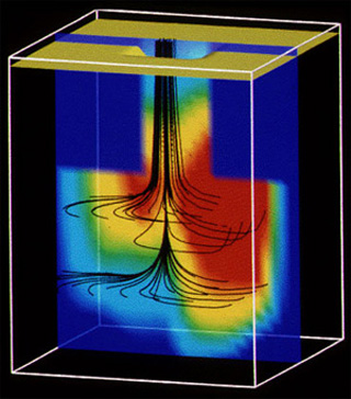
Current flow in a bipolar transistor is discussed in LEC #7. (Image courtesy of the National Coordination Office for Information Technology Research and Development.)
Instructor(s)
Prof. Caroline Ross
MIT Course Number
3.15
As Taught In
Fall 2006
Level
Undergraduate
Course Description
Course Features
Course Description
This course explores the relationships which exist between the performance of electrical, optical, and magnetic devices and the microstructural characteristics of the materials from which they are constructed. The class uses a device-motivated approach which emphasizes emerging technologies. Device applications of physical phenomena are considered, including electrical conductivity and doping, transistors, photodetectors and photovoltaics, luminescence, light emitting diodes, lasers, optical phenomena, photonics, ferromagnetism, and magnetoresistance.
Other Versions
Other OCW Versions
Archived versions: ![]()


